Services
What I Do.
I collaborate with companies, research institutions, and legal firms facing complex challenges in CMOS and SPAD sensor design, semiconductor IP, and system-level integration. My service approach is unique, blending decades of hands-on design and invention with the critical perspective of a technical expert witness.

Design, analysis, and optimization of imaging CMOS architectures — from pixel physics to analog/digital readout.

Development of single-photon-sensitive arrays, ROICs, and calibration methods for SWIR and visible applications.

Guidance on low-noise front-end design, high-speed ADCs, and system-on-chip sensor integration.

Technical analysis for patent litigation in CMOS and semiconductor circuit design.

Advising startups and research teams through concept validation, IP strategy, and prototyping.
Featured Work
SWIRL | Photon-Counting CMOS & SPAD Sensors
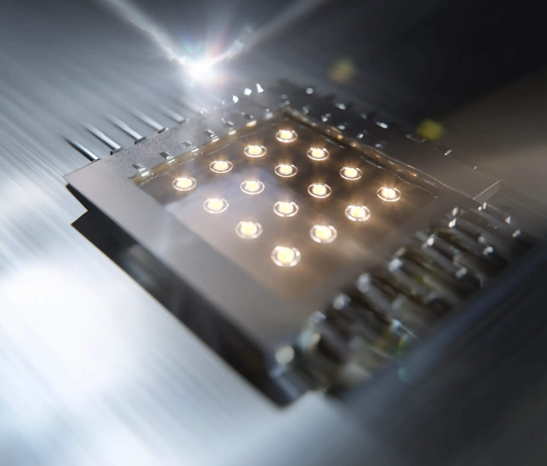
Developing next-generation Single-Photon Avalanche Diode (SPAD) arrays and custom CMOS readout ICs (ROICs) that capture the faintest light in scientific and defense imaging.
Pushing the limits of low-light detection through advanced analog design and photon-counting innovation

Forza Silicon | Entrepreneurial Leadership
Founder and President of Forza Silicon, a leader in custom CMOS image-sensor design, later acquired by AMETEK. Previously held key roles at Photobit, a pioneer in CMOS imaging technology acquired by Micron.
Building companies that bridged cutting-edge sensor technology with commercial success.

NASA JPL | CMOS Camera-on-a-Chip Innovation
As part of the NASA JPL team, contributed to the invention and development of the CMOS camera-on-a-chip — integrating CCD-level performance with CMOS efficiency. Originally created for space exploration, the technology now underpins billions of CMOS cameras used worldwide.
A transformative advancement that made modern digital imaging possible.

